New Technology / Gpu
Monitor GPU demand, AI hardware competition, compute bottlenecks and infrastructure signals shaping the future of machine intelligence.
Unclear topic
Source material: To Accommodate More Computing Power, Data Centers Are Busy Transforming 'Electric' to 'Optical' [Critique Guy]
Summary
Data centers are evolving to enhance computing capabilities by integrating optical communication technologies.
Optical switching improves interconnect efficiency and reduces latency between GPUs.
Challenges remain in scalability and cost efficiency due to centralized architectures.
Innovative solutions like distributed optical switching aim to address these challenges.
Perspectives
The material discusses the transformation of data centers through optical communication technologies.
Proponents of Optical Communication
- Enhance GPU interconnectivity through optical switching
- Reduce latency and improve data transfer efficiency
- Allow for greater scalability in data center architecture
Critics of Current Solutions
- Potential bottlenecks in system design remain unaddressed
Neutral / Shared
- Technological advancements are crucial for improving computing power
- Shared access to GPU resources can enhance overall computing efficiency
- Innovations in data center design are necessary to meet future demands
Metrics
size
5.0 times
size comparison of Cloud Magic 384 super node to NVL72
This indicates a significant increase in computing capacity.
The Cloud Magic 384 super node released by Huawei last year is over 5 times the area of NVL72.
cost
0.0 USD
cost implications of using different GPU brands
Increased costs can hinder the adoption of diverse GPU technologies.
Greatly increased the cost or complexity of data centers
efficiency
0.0 %
inter-GPU communication efficiency
Lower efficiency can impact overall system performance.
scalability
0.0 units
limitations of traditional switches
Limited connections can restrict the growth of data centers.
Each switch can connect a limited number of GPUs
fault_tolerance
0.0 %
system fault tolerance improvements
Enhanced fault tolerance is crucial for large-scale operations.
Greatly enhanced system fault tolerance and stability
growth
0.0 %
growth of computing capabilities
This indicates that advancements in technology can drive growth beyond physical limitations.
The growth of chestnuts is indeed not limited by the size of physical space.
Key entities
Timeline highlights
00:00–05:00
The GB200 airport card is large and consists of 18 EU units, while Huawei's Cloud Magic 384 super node is significantly larger than the NVL72. Enhancements in computing power can be achieved by increasing GPU performance or quantity, but physical limitations in server space and heat dissipation pose challenges.
- The GB200 airport card is large, comparable to a book, and consists of 18 EU units, while the Cloud Magic 384 super node released by Huawei last year is over five times the size of the NVL72, indicating a significant increase in computing power
- To enhance computing power, one can either increase the performance of individual GPUs or the number of GPUs, but typical servers can only accommodate 8 to 12 GPUs due to space and heat dissipation limitations
- Connecting more GPUs requires establishing communication between different servers, forming a shared memory super GPU, known as a super node, but increased scale leads to greater physical distances between GPUs, causing potential communication issues
- In traditional data centers, the distance between two servers can exceed one meter, which can cause latency and signal degradation, similar to delivering documents across cities where efficiency decreases with distance
- Converting electrical signals to optical signals has emerged as a solution, allowing for faster and more efficient communication between servers, enhancing communication speed and reducing interference
- Integrating optical modules with CPU chips minimizes the distance signals must travel, transforming the communication infrastructure and reducing the distance from one meter to just 10 centimeters, which increases interconnect density and improves overall performance
05:00–10:00
The efficiency of GPU collaboration in supernodes is significantly affected by data communication rules and the limitations of traditional electrical switching. Innovations like Google's optical switching aim to enhance inter-GPU communication while addressing cost and scalability challenges.
- The efficiency of GPU collaboration in supernodes is influenced by data communication rules, which dictate how data packets are exchanged and the paths they take, similar to traffic regulations in a city. Traditional switches use electrical signals for routing, which can lead to inefficiencies due to the need for multiple protocols for different GPU brands, increasing costs and complexity
- Google has explored optical switching solutions that keep data in optical form throughout transmission, eliminating the need for conversion to electrical signals and enhancing inter-GPU communication efficiency. However, centralized architectures can lead to increased costs as the number of GPUs grows, since each switch can only connect a limited number of GPUs
- The Docs architecture integrates optical switching capabilities directly into GPUs, allowing for high-speed point-to-point connections without relying on traditional switches. This enhances scalability and reduces costs while improving fault tolerance by enabling dynamic rerouting of data through healthy nodes if a failure occurs
10:00–15:00
The implementation of advanced technologies in data centers enhances the efficient utilization of computing resources, allowing for shared access to GPU resources. This shift towards optical switching improves interconnect efficiency and scalability, driving unprecedented growth in computing capabilities.
- The implementation of advanced technologies allows for more efficient and flexible utilization of computing resources in data centers, enabling shared access to various GPU resources and enhancing overall computing power
- Data centers can achieve unprecedented scalability and adaptability, as the growth of computing capabilities is driven by continuous technological breakthroughs rather than limited physical space
- Innovative solutions like distributed optical switching facilitate effective interconnections for each GPU and node, making supercomputing more attainable through technological advancements
- The transition to optical switching eliminates the need for converting optical signals to electrical signals, significantly improving interconnect efficiency between GPUs
- By allowing GPUs to interconnect directly without traditional switches, the distributed optical switching architecture enhances system scalability and fault tolerance
NVIDIA H200 GPU Export to China
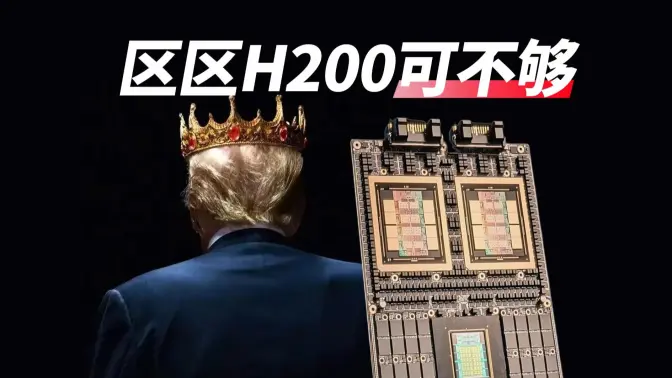
Source material: The H200 is Not Enough, the Initiative is Changing
Summary
The Trump administration is considering the export of the NVIDIA H200 GPU to China.
The H200 features upgrades over the H100 but lags behind the B200 in communication technology.
Concerns about national security and technological espionage are significant.
The export could inadvertently enhance China's AI capabilities.
Perspectives
Discussion focuses on the implications of exporting AI technology.
Support for Exporting H200
- Consider exporting H200 as it has notable upgrades over H100
- Facilitate collaboration with China on AI technology
Opposition to Exporting H200
- Highlight national security risks associated with the export
- Emphasize potential strengthening of Chinas AI capabilities
Neutral / Shared
- Acknowledge the technological advancements of the H200 GPU
- Recognize the competitive landscape in AI chip production
Metrics
power_consumption
600.0 kW
power consumption of a specific GPU
High power consumption raises concerns about energy efficiency in AI operations.
Its power consumption is as high as 600 kilowatts.
Key entities
Timeline highlights
00:00–05:00
The Trump administration is contemplating the export of the NVIDIA H200 GPU to China, which raises questions about its implications. The H200 GPU has notable upgrades over the H100, but still falls short compared to the B200 in communication technology.
- The Trump administration is considering approving the export of the new NVIDIA H200 GPU to China, raising questions about whether this is beneficial or merely a test of limits
- The H200 GPU features significant upgrades over the H100, particularly in memory and bandwidth, but it still lags behind the B200 in terms of communication technology
- Despite the H100 being available since 2023, there is still a backlog for orders in the U.S., with many companies waiting until late 2024 for delivery, indicating a supply chain issue
- The B300 GPU has faced delays due to production challenges at TSMC, making the availability of the H200 a timely opportunity for some
- The discussion around AI chips has shifted, with companies like Google proving that strong models can be trained without relying on large ecosystems, highlighting a change in the competitive landscape
- The cost of achieving similar computational power is becoming a critical factor, as the efficiency of AI chip production and energy consumption will determine the competitive edge between nations
Unclear topic
Source material: It's 2026, why is ASML still researching the 'previous generation' DUV? [Silicon Valley 101]
Summary
ASML's DUV technology remains crucial in chip production, accounting for a significant portion of the manufacturing process.
Despite advancements in EUV technology, DUV machines are more efficient and cost-effective for many applications.
ASML continues to innovate within the DUV space to enhance production capabilities and meet market demands.
The integration of DUV technology with advanced lithography solutions creates a positive feedback loop in chip manufacturing.
Perspectives
Focus on the significance of DUV technology in the semiconductor industry.
Support for DUV Technology
- Emphasizes DUVs role in producing 90% of advanced chips
- Highlights DUVs cost-effectiveness compared to EUV
- Points out DUVs efficiency in handling multiple chip layers
Advocacy for EUV Technology
- Argues for the potential of EUV to revolutionize chip manufacturing
- Raises concerns about the long-term viability of DUV as technology evolves
Neutral / Shared
- Acknowledges the ongoing innovation in DUV technology
- Recognizes the importance of balancing DUV and EUV in production
- Notes the challenges associated with 3D chip integration
Metrics
production_efficiency
400.0 units
DUV machine exposure rate
Higher exposure rates lead to increased production efficiency.
This is the highest output DUV lithography, capable of exposing over 400 wafers per hour.
production_efficiency
220.0 units
EUV machine exposure rate
Lower exposure rates in EUV machines limit their production capacity.
This is currently the highest output EUV lithography, exposing up to 220 wafers per hour.
market_share
90.0 %
DUV's share in advanced chip production
A significant market share indicates DUV's critical role in chip manufacturing.
DUV's performance can even reach ninety percent.
exposure_area
4.0 units
exposure area of the ThingsGAN XT 260 compared to traditional machines
This increase in exposure area can significantly reduce production time and costs.
Provides four times the market of traditional methods
throughput
400.0 units
wafers produced per hour
Higher throughput indicates improved efficiency in chip manufacturing.
Can increase the output of sutras to over 400 pieces in less than an hour.
Key entities
Timeline highlights
00:00–05:00
The production of advanced three-nanometer chips still heavily relies on older DUV machines, which account for up to 90% of chip manufacturing. Despite the introduction of EUV technology, DUV remains essential due to its cost-effectiveness and efficiency in producing various chip layers.
- Most of the latest three-nanometer chips in smartphones are still produced using older DUV machines, highlighting the ongoing relevance of DUV in chip manufacturing
- ASMLs DUV machines produce the majority of chips globally, including those made with EUV technology, as even the most advanced chips rely on DUV for many of their layers
- DUV remains the dominant technology in chip production, accounting for up to 90% of advanced chip manufacturing, indicating its continued importance in the mainstream market
- The production cost is a significant factor preventing a complete shift to EUV, as DUV machines can expose over 400 wafers per hour compared to the 220 wafers of the most efficient EUV machines
- Many chips, such as automotive and memory chips, prioritize cost and stability over extreme precision, further solidifying DUVs position in the market
- There is still potential for innovation in DUV technology, especially with the shift towards 3D chip stacking, which allows for vertical growth in chip design
05:00–10:00
3D integration in chip manufacturing involves stacking multiple chips vertically, which presents challenges such as alignment precision and structural stability. ASML's innovations, including the ThingsGAN XT 260 lithography machine, aim to enhance production efficiency and accuracy in this complex process.
- 3D integration in chip manufacturing involves stacking multiple chips vertically, presenting challenges such as alignment precision and structural stability. ASML optimizes lithography processes to facilitate this integration, focusing on the K1 factor for improvements
- Overlay accuracy is critical for the alignment of multi-layer chips, and enhancements can be achieved through stable materials and optimized processes. ASML has established a department dedicated to achieving high flatness in lithography equipment, essential for precise imaging
- ASMLs ThingsGAN XT 260 lithography machine is designed for advanced packaging, offering significant improvements in exposure capabilities. It provides four times the exposure area compared to traditional machines, reducing the need for stitching and enhancing production efficiency
10:00–15:00
ASML's acquisition of Hermes Microwation in 2016 for approximately 2.75 billion euros has proven beneficial for their lithography solutions. The core requirements in chip mass production include precise measurement and rapid inspection to ensure quality and performance.
- In 2016, ASML acquired Hermes Microwation for approximately 2.75 billion euros, a deal that was 30% above the market price at the time, proving beneficial as it became a crucial part of their holistic lithography solution
- The core requirements in chip mass production are measurement and inspection, with measurement focusing on precise values and inspection quickly scanning for physical defects
- To enhance overlay accuracy, ASML employs a feedback loop where measurement data from previous layers dynamically adjusts exposure parameters for subsequent layers, similar to a marksman adjusting their aim
- ASML has transitioned from optical inspection tools to electron beam inspection tools for higher precision, although the latter are slower than optical methods
- ASML is upgrading electron beam inspection tools to improve detection speed, which is crucial for maintaining efficiency in chip manufacturing
- In 2D microfabrication, the challenges of DUV technology are increasing as circuit sizes shrink, prompting the adoption of new design techniques to enhance transistor density
15:00–20:00
ASML's Tunescan NXP870B has improved throughput to over 400 wafers per hour, enhancing production efficiency. The company continues to invest in DUV technology to meet market demand and improve precision in chip production.
- ASMLs latest Tunescan NXP870B has upgraded optical components, increasing throughput to over 400 wafers per hour, significantly enhancing production efficiency
- The integration of computational lithography and metrology tools creates a positive feedback loop, optimizing chip manufacturing processes
- ASML continues to invest in DUV technology due to persistent market demand and its ability to improve both precision and throughput in chip production
- DUV technology supports 3D integration by enhancing precision and contributes to economic efficiency through increased production yields
- ASMLs strategy involves a dual approach where the DUV route safeguards chip production while the EUV route explores future lithography advancements